高速信号过孔仿真的三种方法
“ 在多层PCB/封装基板的设计中,会有非常多的过孔连接。低频情况下,过孔不影响信号传输。然而,随着频率上升(GHz级)和信号上升沿变得陡峭(ns级),此时的过孔不能简单地视为电气连接,而必须考虑过孔对信号完整性的影响。本文介绍了三种用于高速信号过孔仿真的方法,借助的工具分别为:HFSS Via Wizard、ADS Via Designer以及HyperLynx LineSim 。” 关键词:高速信号,过孔设计,HFSS,ADS,HyperLynx
01
过孔的影响
过孔带来的问题主要集中在寄生电容和寄生电感上。寄生电容会延长信号的上升时间,降低电路的运行速率。寄生电感会削弱旁路电容的作用,降低系统的滤波性能。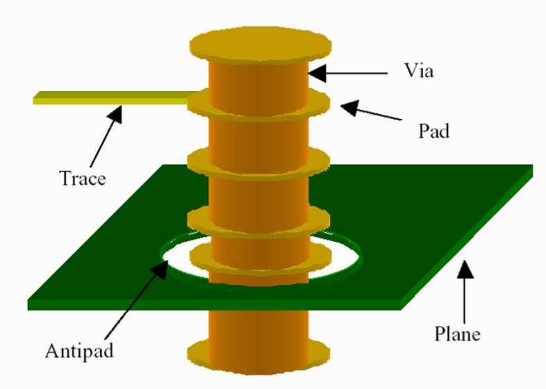
信号延迟主要来自过孔的寄生电容,通过下式计算:
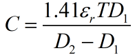
其中,D2为接地焊盘(阻焊区)直径(mm),D1为过孔焊盘直径(mm),T为PCB板厚度(mm),εr为基板介电常数,C为过孔的寄生电容(pF)。
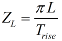
信号的上升时间通过下式计算:
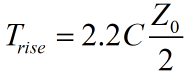
其中,Z0为传输线阻抗,Trise为信号的上升时间(10%-90%)。
过孔的寄生电感,可由下式计算:
其中,L表示过孔的寄生电感 (nH),h表示过孔的长度 (mm),d表示过孔的直径 (mm)。
由过孔寄生电感引起的等效阻抗变化,可由下式计算:
02
HFSS Via Wizard
Via Wizard是一款针对HFSS开发的建模小工具,大小只有2MB不到,可以快速生成3D过孔模型。它建模的主要原理是:在该工具的安装路径下生成一个.vbs文件(根据用户在软件UI界面中设置的参数生成),然后HFSS调用该文件去完成建模。了解Ansys自动化建模的同学,听起来是不是很熟悉?讲这个原理的目的是,如果有同学在用Via Wizard这款插件时,遇到无法生成模型的情况,可以在HFSS中手动调用该.vbs文件进行建模。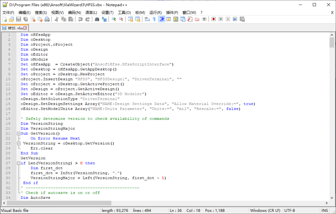
社长以前给公司做过一些Python-Ansys的仿真自动化/二次开发项目,感兴趣的同学可以一起交流学习。以下,进行该插件的常规流程演示,可视化操作较为简单,略有删减。
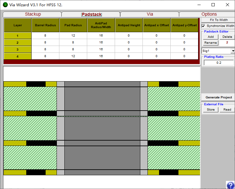
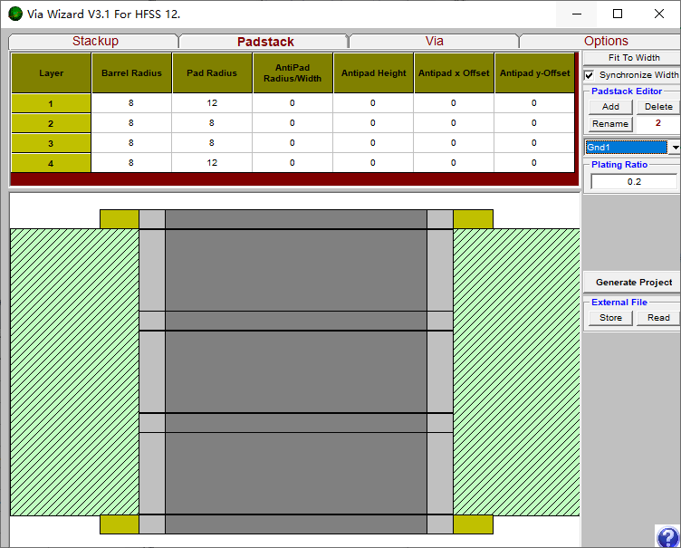
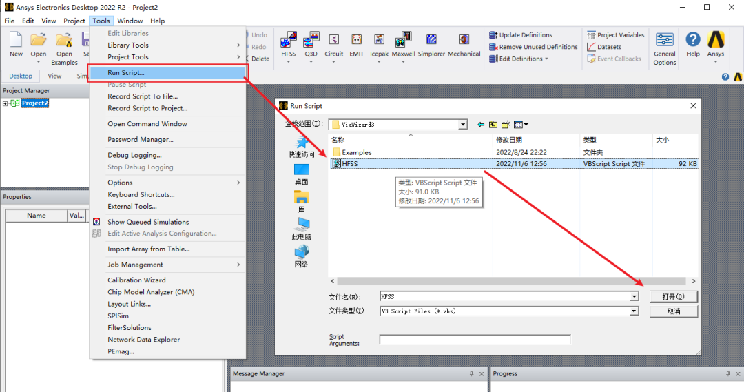
- 在Via Wizard完成设置后,便可Generate生成HFSS中的信号过孔模型。同时该插件还会自动将过孔相关的尺寸设为变量,这样参数化处理之后更方便我们后续对过孔进行优化设计。HFSS中的仿真设置,在此不赘述。
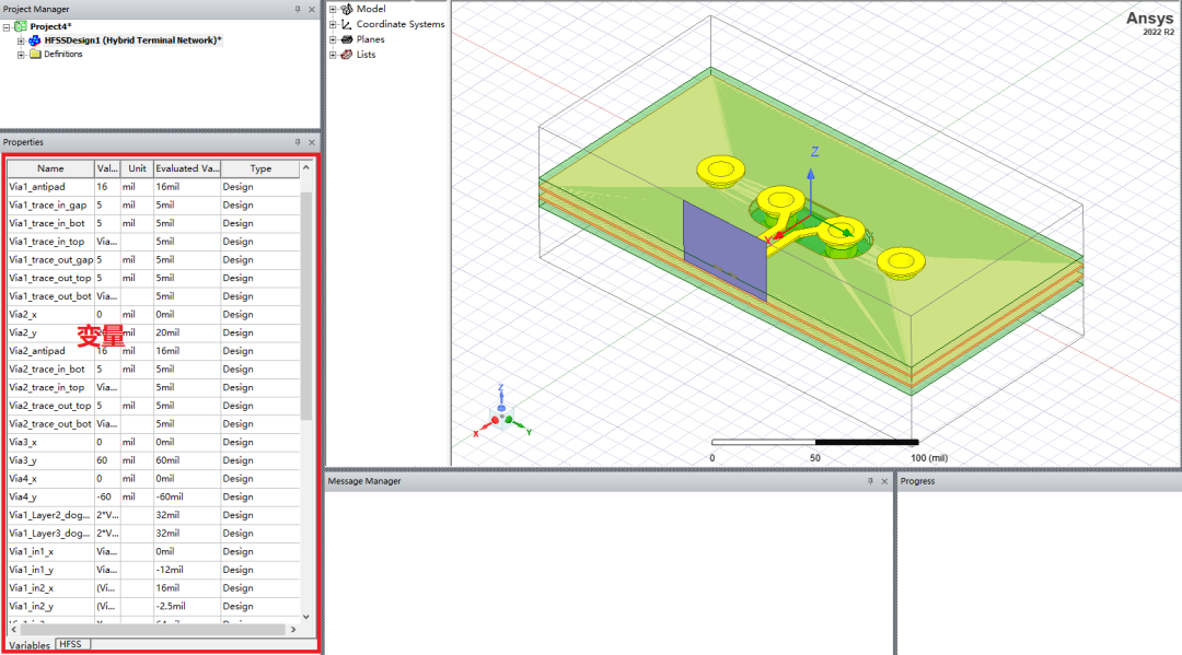
Via(num)_x
The x-location of the via center The y-location of the via center The width of the lower section of the trapezoidal trace into the via The width of the upper section of the trapezoidal trace into the via The width of the lower section of the trapezoidal trace out of the via The width of the upper section of the trapezoidal trace out of the via The width of the lower section of the trapezoidal trace into the via The depth of copper that is removed from the bottom of the viaLocation of x points for trace into the via Location of y points for trace into the via Location of x points for trace out of the via Location of y points for trace out of the via For Differential Vias Only The spacing between the differential traces into the via The spacing between the differential traces out of the via Via(num)_Layer(num)_dogbone The height of the rectangular clearance between differential vias Conductor thickness of that layer Dielectric thickness of that layer Elevation in Z-direction of bottom of conductor Elevation in Z-direction of bottom of dielectricMinimum X dimensions of project Length of X dimensions of projectMinimum Y dimensions of project Length of Y dimensions of projectMinimum Z dimensions of project including Airbox Length of Z dimensions of project including Airbox This variable is created only if antipads are identical on all layers. This variable will control the antipad dimensions on all layers Via(num)_Layer(num)_antipadVia(num)_Layer(num)_antipad_height Via(num)_Layer(num)_Antipad_x_offset Antipad registration in X direction Via(num)_Layer(num)_Antipad_y_offset Antipad registration in Y direction Via(num)_Layer(num)_Antipad_xmin Used as starting point for rectangular antipads. Computed from other variables Via(num)_Layer(num)_Antipad_ymin Used as starting point for rectangular antipads. Computed from other variables Via(num)_Layer(num)_Antipad_x_center Used as starting point for circular antipads. Computed from other variables Via(num)_Layer(num)_Antipad_y_center Used as starting point for circular antipads. Computed from other variables Via(num)_Layer(num)_Antipad_x_center Used as starting point for circular antipads. Computed from other variables Defines Y location of left edge of WavePortIn Defines Y location of right edge of WavePortIn Defines Y location of left edge of WavePortOut Defines Y location of right edge of WavePortOut03
ADS Via Designer
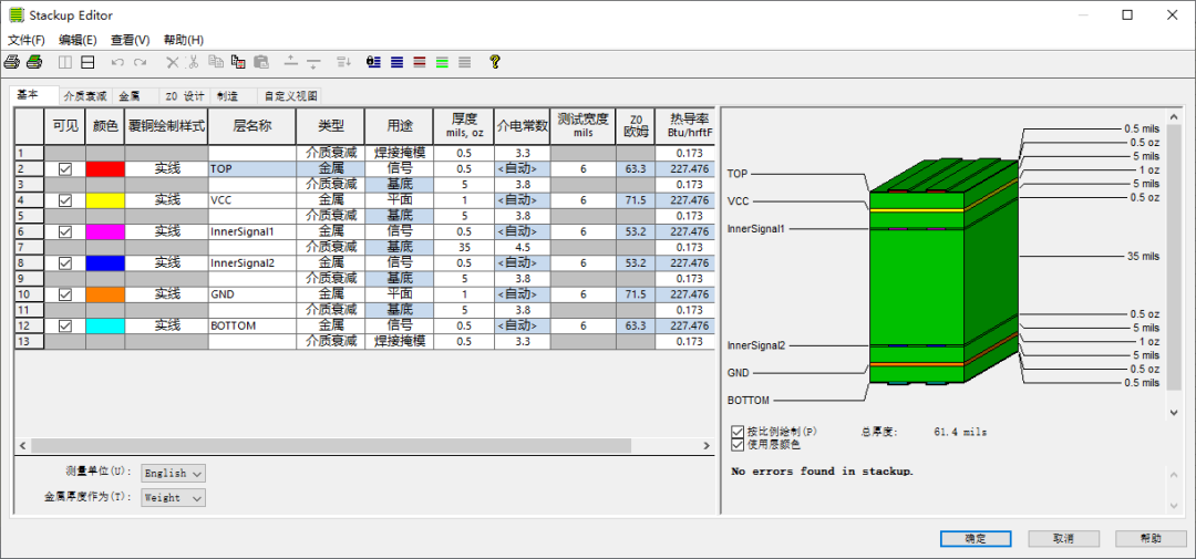
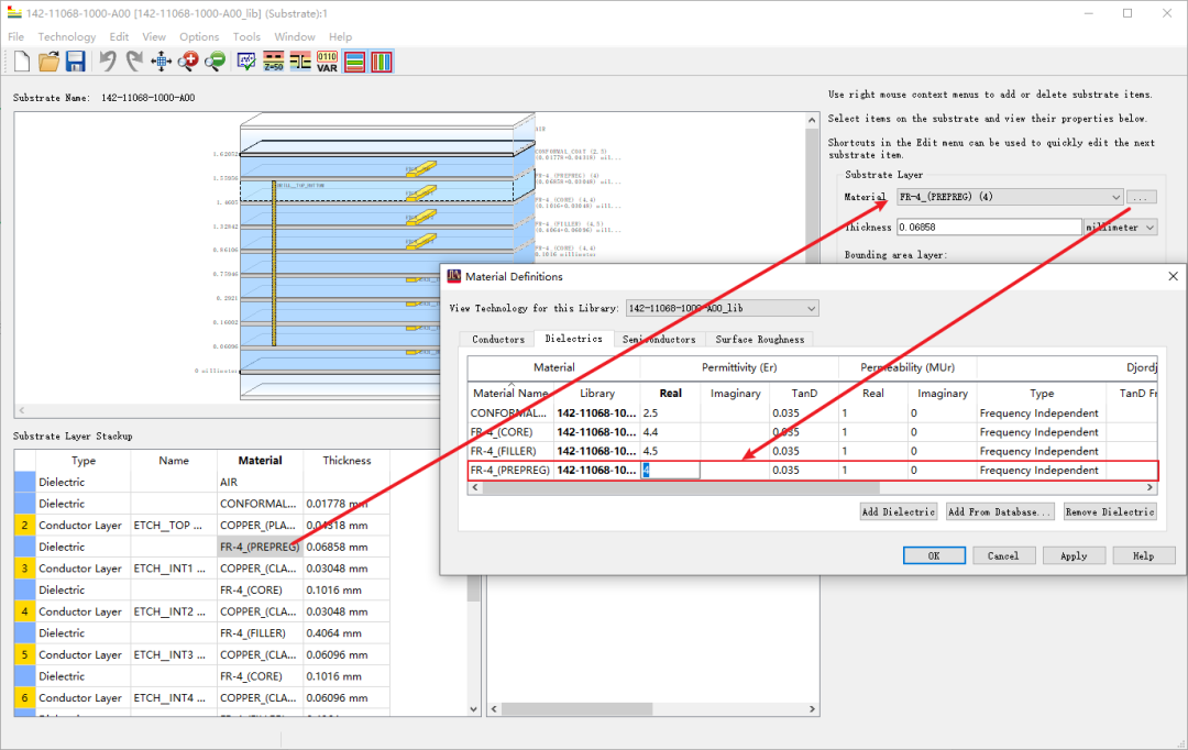
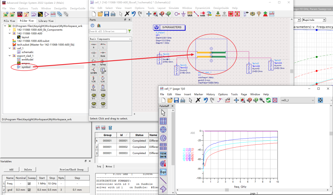
在ADS中进行过孔设计时,如果尚未进行Layout,那么叠层可以自己定义。如果已经有叠层信息了,建议直接将PCB文件导入ADS中,省去建叠层的过程。
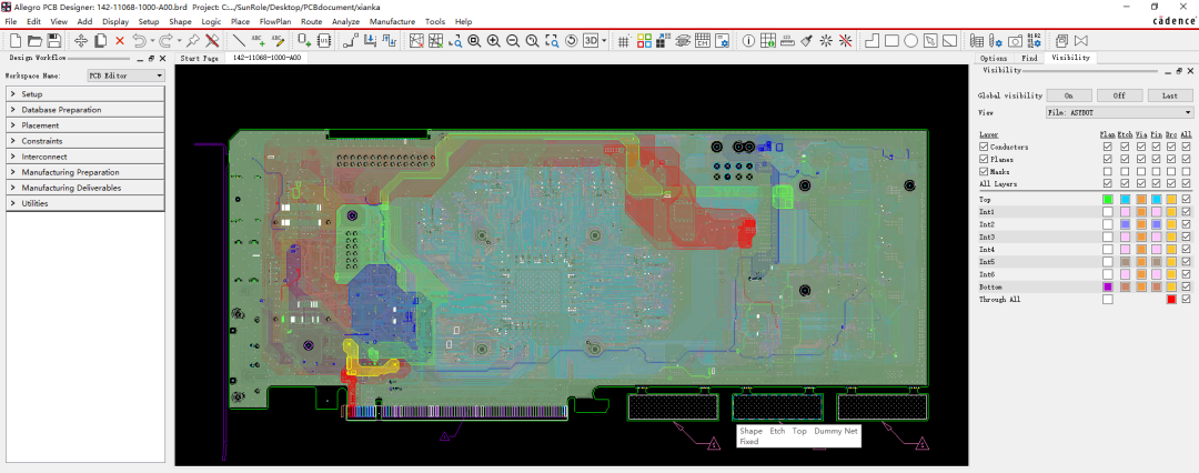
▲本例中使用的NVIDIA显卡PCB文件[2010年产品]
- 叠层信息核对,Dk/Df值应与厂家保持一致。互连工程师会保证自己所画PCB物理尺寸的正确,但一般不会花时间去给你填板材电参数的实际值,这里切记要检查。
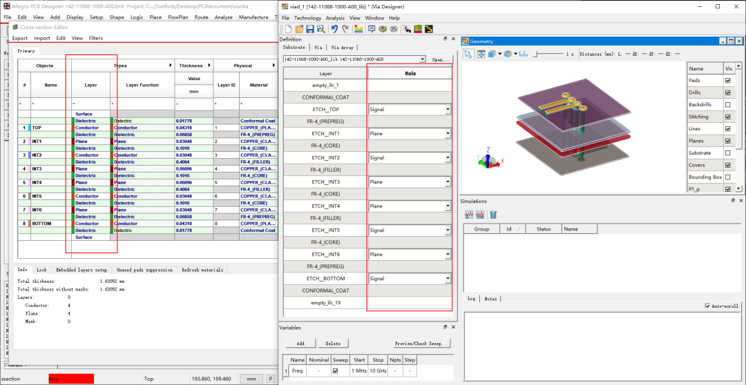
- 打开Via Designer,首先根据Allegro PCB的Layer Function修改Via Designer中的Layer Role。
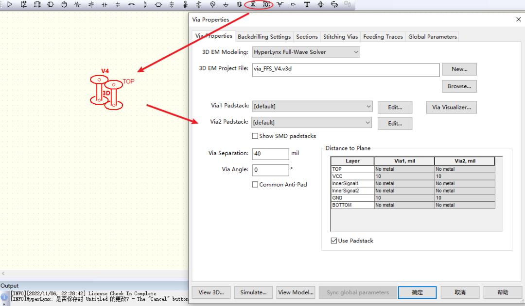
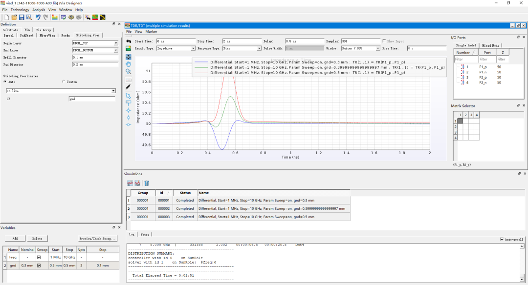
- 同样地,如果要对某个参数进行扫参优化设计,将其设为变量,设置取值范围。我们以地孔(缝合孔)为例,看该参数对结果的影响,将其设为gnd=0.3,0.4,0.5。
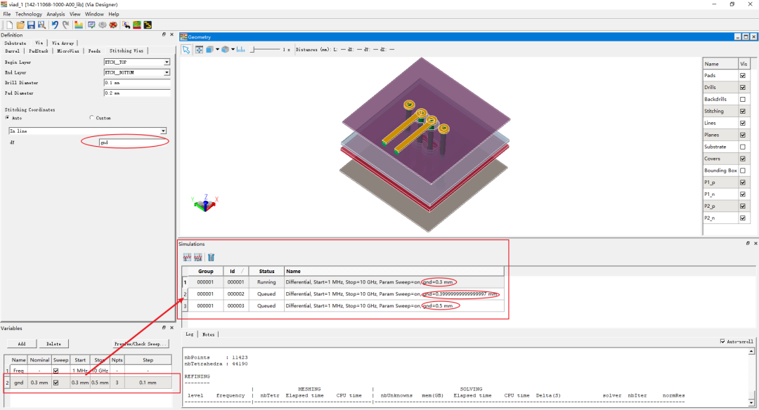
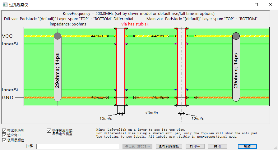
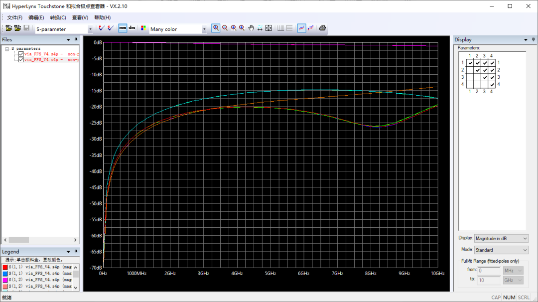
- 不同变量下的仿真结果:单端、差分形式的S参数及TDR阻抗。
04
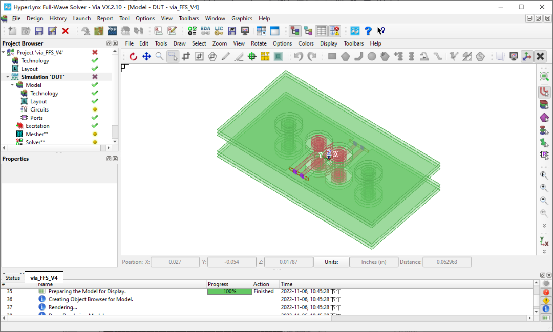
HyperLynx LineSim
使用HyperLynx进行建模与ADS有类似之处,不过相比前面介绍的两种,使用HyperLynx显得更加小众一些。分析可能的原因在于,前两者具有更高的与其他软件(仿真格式)进行联仿的兼容性。